- 您现在的位置:买卖IC网 > Sheet目录312 > AT26DF081A-SSU (Atmel)IC FLASH 8MBIT 70MHZ 8SOIC
�� �
�
�9.2�
�Write� Disable�
�The� Write� Disable� command� is� used� to� reset� the� Write� Enable� Latch� (WEL)� bit� in� the� Status� Reg-�
�ister� to� the� logical� “0”� state.� With� the� WEL� bit� reset,� all� program,� erase,� Protect� Sector,� Unprotect�
�Sector,� and� Write� Status� Register� commands� will� not� be� executed.� The� Write� Disable� command�
�is� also� used� to� exit� the� Sequential� Program� Mode.� Other� conditions� can� also� cause� the� WEL� bit�
�to� be� reset;� for� more� details,� refer� to� the� WEL� bit� section� of� the� Status� Register� description.�
�To� issue� the� Write� Disable� command,� the� CS� pin� must� first� be� asserted� and� the� opcode� of� 04h�
�must� be� clocked� into� the� device.� No� address� bytes� need� to� be� clocked� into� the� device,� and� any�
�data� clocked� in� after� the� opcode� will� be� ignored.� When� the� CS� pin� is� deasserted,� the� WEL� bit� in�
�the� Status� Register� will� be� reset� to� a� logical� “0”.� The� complete� opcode� must� be� clocked� into� the�
�device� before� the� CS� pin� is� deasserted,� and� the� CS� pin� must� be� deasserted� on� an� even� byte�
�boundary� (multiples� of� eight� bits);� otherwise,� the� device� will� abort� the� operation� and� the� state� of�
�the� WEL� bit� will� not� change.�
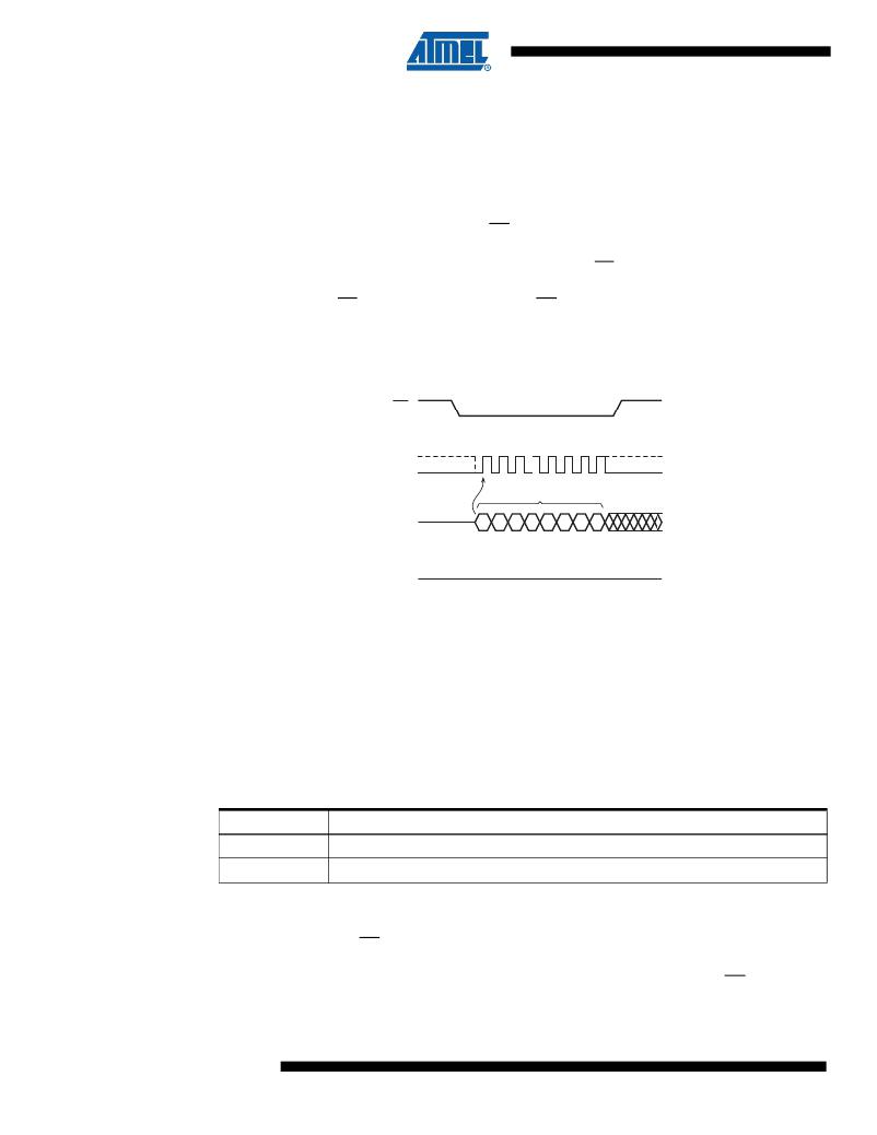
�Figure� 9-2.�
�Write� Disable�
�C� S�
�0�
�1�
�2�
�3�
�4�
�5�
�6�
�7�
�S� CK�
�OPCODE�
�S� I�
�0�
�0�
�0�
�0�
�0�
�1�
�0�
�0�
�M� S� B�
�S� O�
�HIGH-IMPEDANCE�
�9.3�
�Protect� Sector�
�Every� physical� sector� of� the� device� has� a� corresponding� single-bit� Sector� Protection� Register�
�that� is� used� to� control� the� software� protection� of� a� sector.� Upon� device� power-up� or� after� a�
�device� reset,� each� Sector� Protection� Register� will� default� to� the� logical� “1”� state� indicating� that� all�
�sectors� are� protected� and� cannot� be� programmed� or� erased.�
�Issuing� the� Protect� Sector� command� to� a� particular� sector� address� will� set� the� corresponding�
�Sector� Protection� Register� to� the� logical� “1”� state.� The� following� table� outlines� the� two� states� of�
�the� Sector� Protection� Registers.�
�Table� 9-1.�
�Value�
�0�
�1�
�Sector� Protection� Register� Values�
�Sector� Protection� Status�
�Sector� is� unprotected� and� can� be� programmed� and� erased.�
�Sector� is� protected� and� cannot� be� programmed� or� erased.� This� is� the� default� state.�
�Before� the� Protect� Sector� command� can� be� issued,� the� Write� Enable� command� must� have� been�
�previously� issued� to� set� the� WEL� bit� in� the� Status� Register� to� a� logical� “1”.� To� issue� the� Protect�
�Sector� command,� the� CS� pin� must� first� be� asserted� and� the� opcode� of� 36h� must� be� clocked� into�
�the� device� followed� by� three� address� bytes� designating� any� address� within� the� sector� to� be�
�locked.� Any� additional� data� clocked� into� the� device� will� be� ignored.� When� the� CS� pin� is� deas-�
�serted,� the� Sector� Protection� Register� corresponding� to� the� physical� sector� addressed� by�
�A23� -� A0� will� be� set� to� the� logical� “1”� state,� and� the� sector� itself� will� then� be� protected� from�
�16�
�AT26DF081A�
�3600G–DFLASH–06/09�
�发布紧急采购,3分钟左右您将得到回复。
相关PDF资料
AT26DF161-SU
IC FLASH 16MBIT 66MHZ 8SOIC
AT26DF161A-MU
IC FLASH 16MBIT 70MHZ 8QFN
AT26DF321-SU
IC FLASH 32MBIT 66MHZ 8SOIC
AT27BV010-90JU
IC OTP 1MBIT 90NS 32PLCC
AT27BV020-90JU
IC OTP 2MBIT 90NS 32PLCC
AT27BV040-12JU
IC OTP 4MBIT 120NS 32PLCC
AT27BV1024-90JU
IC OTP 1MBIT 90NS 44PLCC
AT27BV256-70JU
IC OTP 256KBIT 70NS 32PLCC
相关代理商/技术参数
AT26DF081A-SSU-RET
制造商:Atmel Corporation 功能描述:
AT26DF081A-ST-B
制造商:Adesto Technologies Corporation 功能描述:8-SOIC-W, AUTO GRADE 3, 2.7V, TUBE - Rail/Tube
AT26DF081A-ST-T
制造商:Adesto Technologies Corporation 功能描述:8-SOIC-W, AUTO GRADE 3, 2.7V, T&R - Tape and Reel
AT26DF081A-SU
功能描述:闪存 8M 8 I/O Pins SPI 256B 2.7V-3.6V RoHS:否 制造商:ON Semiconductor 数据总线宽度:1 bit 存储类型:Flash 存储容量:2 MB 结构:256 K x 8 定时类型: 接口类型:SPI 访问时间: 电源电压-最大:3.6 V 电源电压-最小:2.3 V 最大工作电流:15 mA 工作温度:- 40 C to + 85 C 安装风格:SMD/SMT 封装 / 箱体: 封装:Reel
AT26DF081-MU
制造商:Adesto Technologies Corporation 功能描述:SF DATAFLASH, 8M, MLF, IND TEMP,GREEN - Trays
AT26DF081-SU
制造商:Adesto Technologies Corporation 功能描述:SF DATAFLASH, 8M, SOIC ,IND TEMP, GREEN - Rail/Tube
AT26DF161
制造商:ATMEL 制造商全称:ATMEL Corporation 功能描述:16-megabit 2.7-volt Only Serial Firmware DataFlash Memory
AT26DF161_06
制造商:ATMEL 制造商全称:ATMEL Corporation 功能描述:16-megabit 2.7-volt Only Serial Firmware DataFlash Memory